Team:ETH Zurich/lab/chip
From 2014.igem.org
(→Overview) |
(→Overview) |
||
| Line 8: | Line 8: | ||
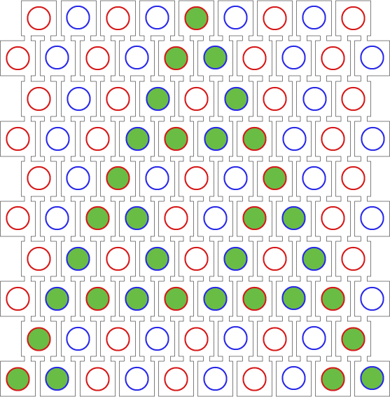
[[File:ETH_Zurich_2014_theoretical_grid.png|210px|thumb|left|Outline of a PDMS-made grid loaded with cells confined in alginate beads for the biological implementation of cellular automata (ON state=sfGFP/green, OFF state=white).]] | [[File:ETH_Zurich_2014_theoretical_grid.png|210px|thumb|left|Outline of a PDMS-made grid loaded with cells confined in alginate beads for the biological implementation of cellular automata (ON state=sfGFP/green, OFF state=white).]] | ||
| + | |||
| + | In the following, we have investigated the combination of additive manufacturing (3D-printing) and PDMS chip fabrication for applications in synthetic biology. This rapid prototyping approach allowed us to update our chips continuously according to new insights from modeling or the wet lab and in particular to avoid more intricate photolitographic approaches, which generally require clean room access, relatively expensive raw materials, and in depth knowledge of etching techniques. | ||
<br> | <br> | ||
<br> | <br> | ||
| - | + | As a result, we are convinced that the tinkering with 3D-printing for mold creation is more economical for our applications and perfectly in line with the do-it-yourself spirit of iGEM. | |
| - | + | ||
| - | + | ||
| - | + | ||
| - | + | ||
| - | + | ||
| - | + | ||
| - | + | ||
<html></article></html> | <html></article></html> | ||
Revision as of 14:30, 16 October 2014
Millifluidic Chip & Rapid Prototyping
Overview
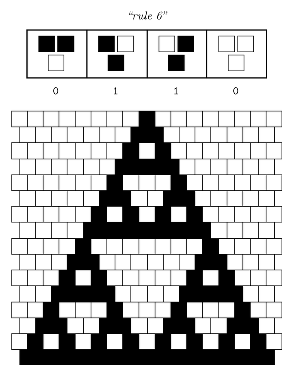
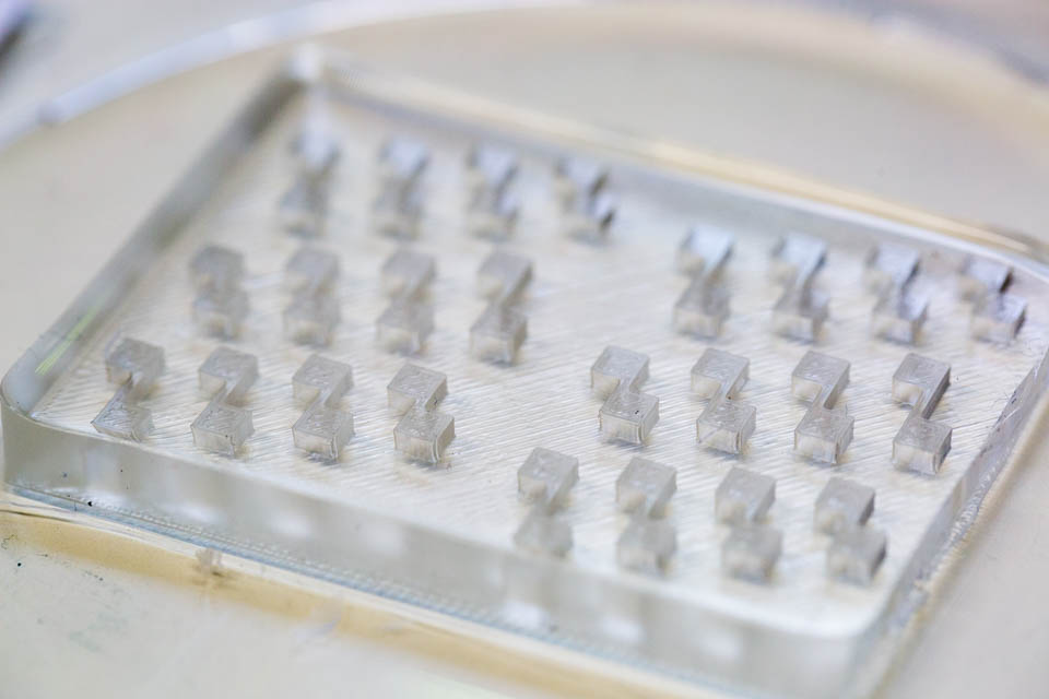
Our project aims for the biological implementation of cellular automata, so we had to find a way to create a regular grid of cells with a defined neighborhood as shown in the pictures below. On the left side a classical cellular automata is depicted, on the right side an outline of our biological version consisting of a grid-like polydimethylsiloxane (PDMS) chip filled with cell colonies encapsulated in alginate beads.
In the following, we have investigated the combination of additive manufacturing (3D-printing) and PDMS chip fabrication for applications in synthetic biology. This rapid prototyping approach allowed us to update our chips continuously according to new insights from modeling or the wet lab and in particular to avoid more intricate photolitographic approaches, which generally require clean room access, relatively expensive raw materials, and in depth knowledge of etching techniques.
As a result, we are convinced that the tinkering with 3D-printing for mold creation is more economical for our applications and perfectly in line with the do-it-yourself spirit of iGEM.
Mold Design and 3D Print Exchange
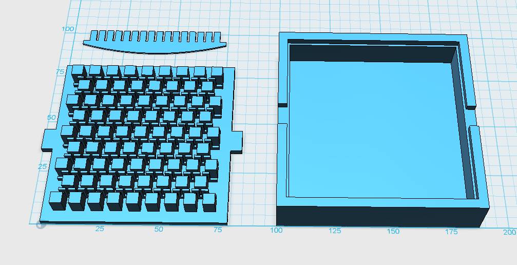
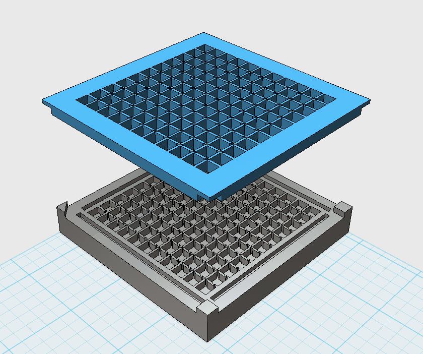
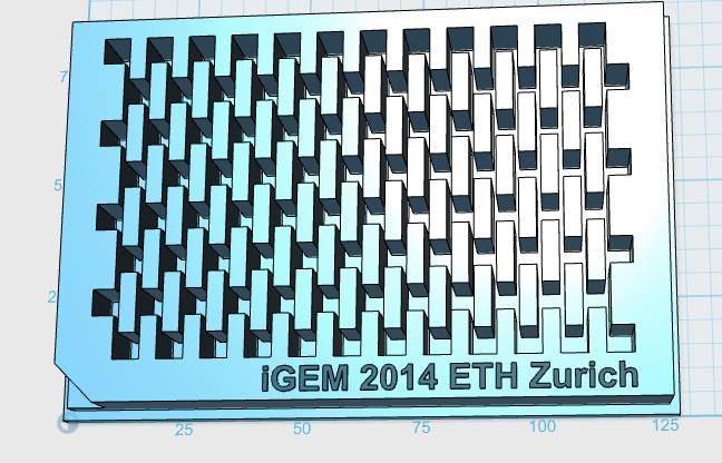
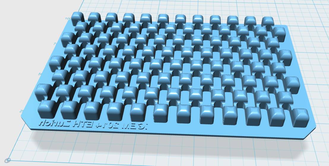
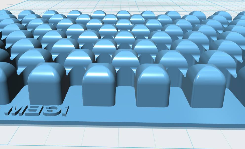
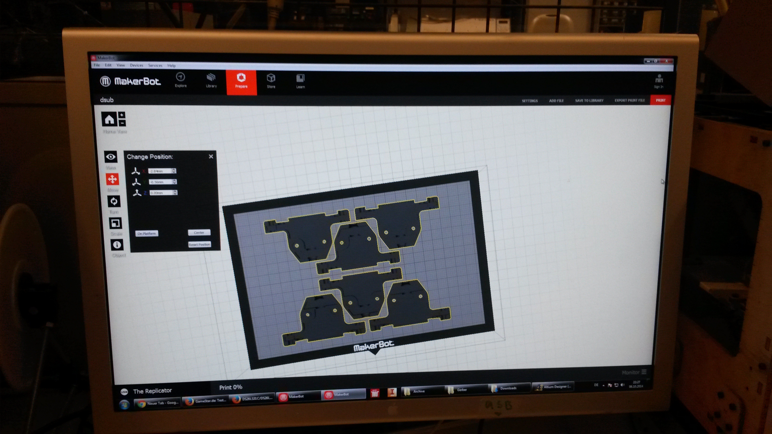
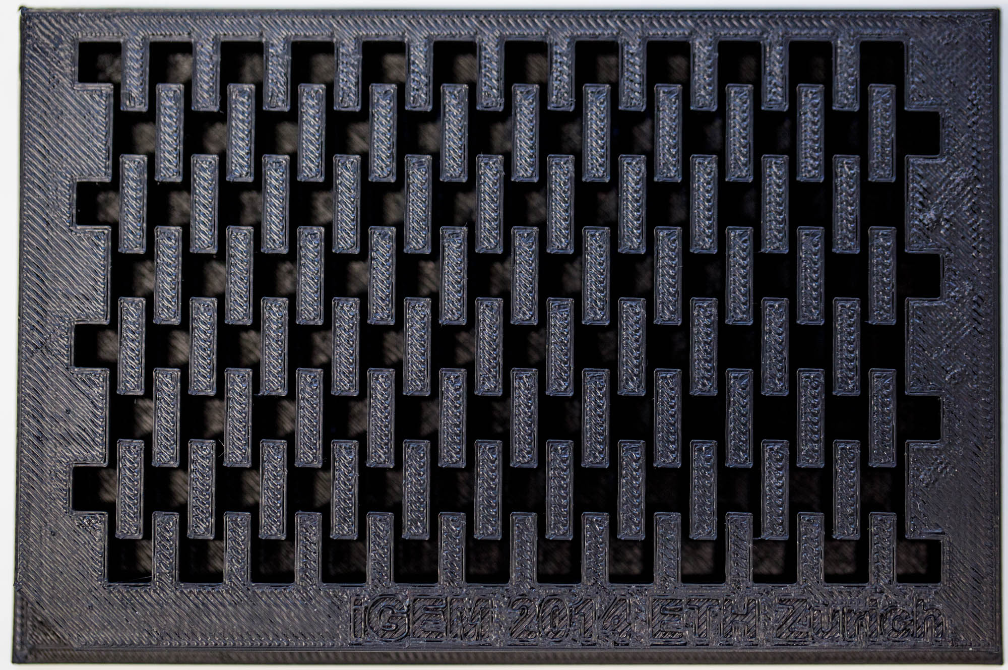
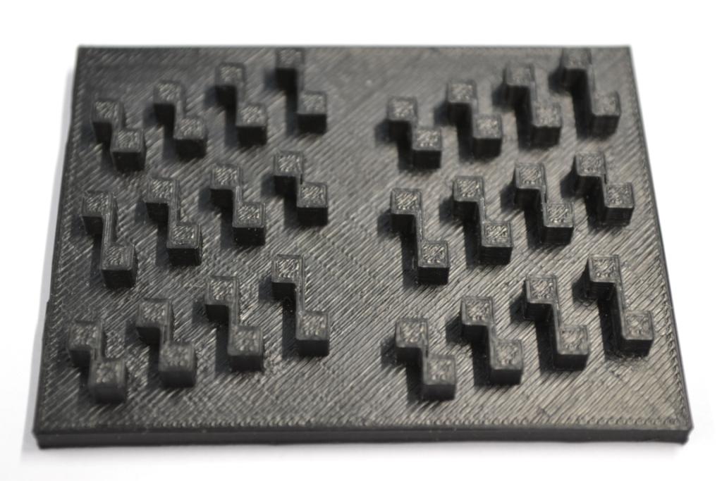
Our custom-made plates and molds were design using a common personal computer (MacBook Air, 13-inch, early 2014, 1.7 GHz Intel Core i7, 8 GB 1600 MHz) and a 3D computer aided design (CAD) software package that is freely available for Mac OS X 10.9.4 ([http://www.123dapp.com/design Autodesk123D Design]). The CAD models were exported as mesh files (.stl) to the 3D printer's software ([http://www.makerbot.com/support/makerware/troubleshooting/ MakerWare]). The dimensions of the device-structures were usually between 1 mm and 5 mm, falling in the range of millifluidics.
3D-Printing and Rapid Prototyping
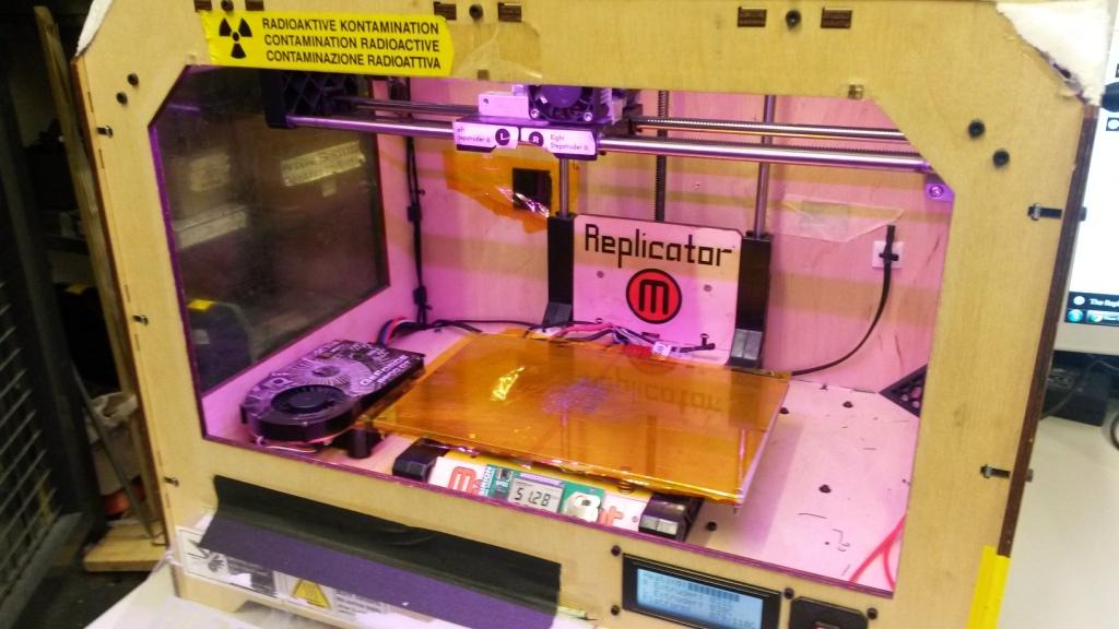
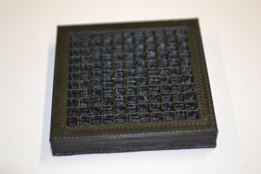
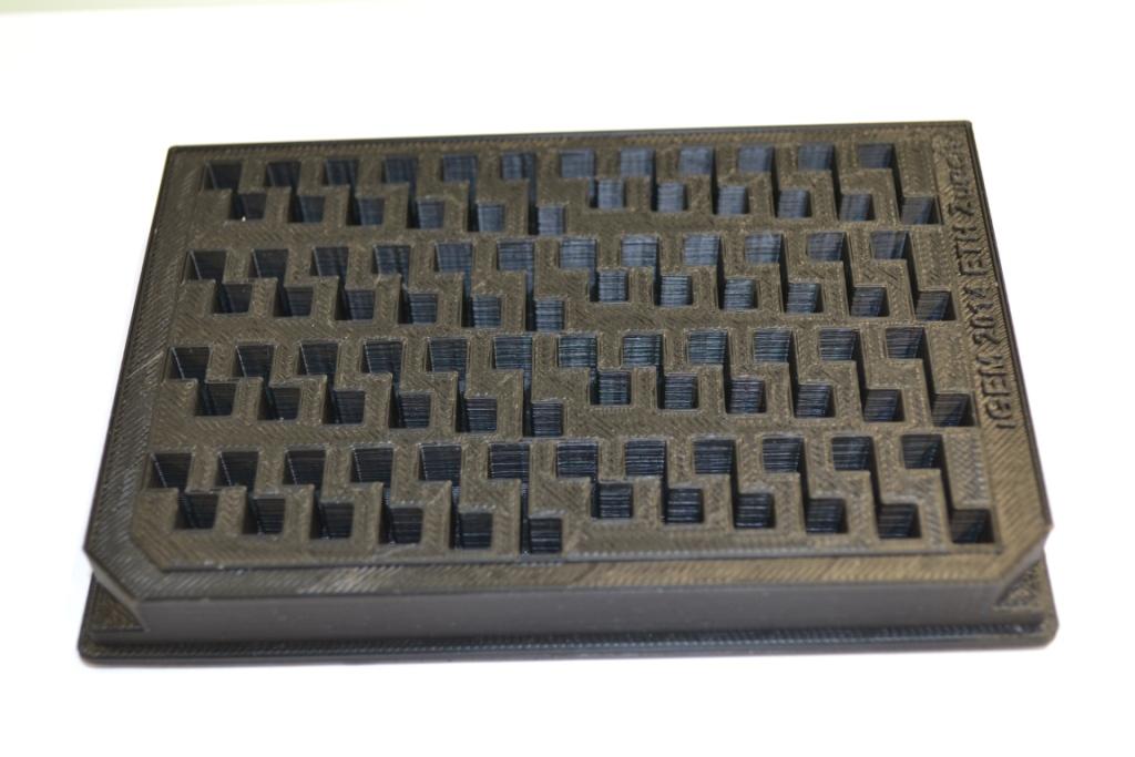
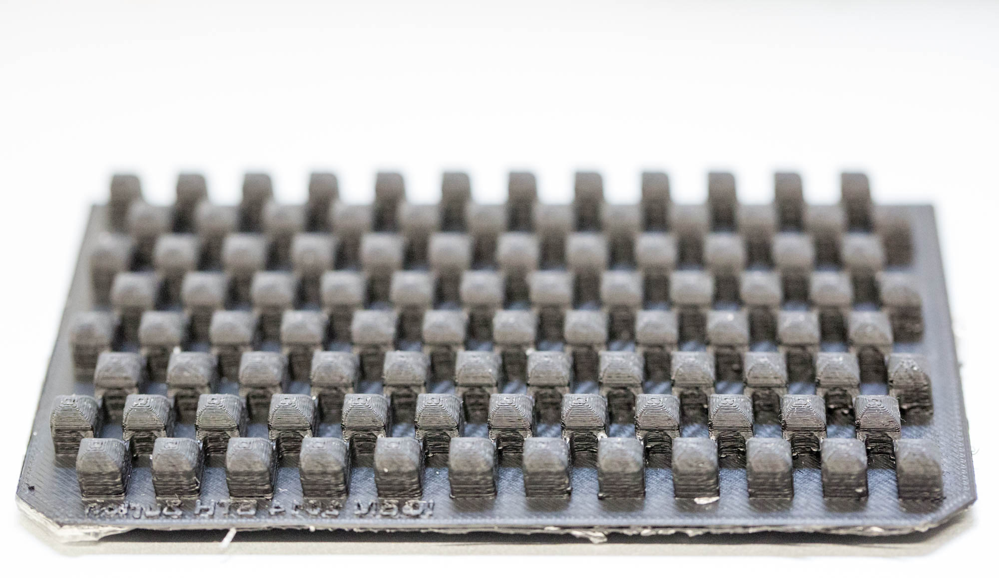
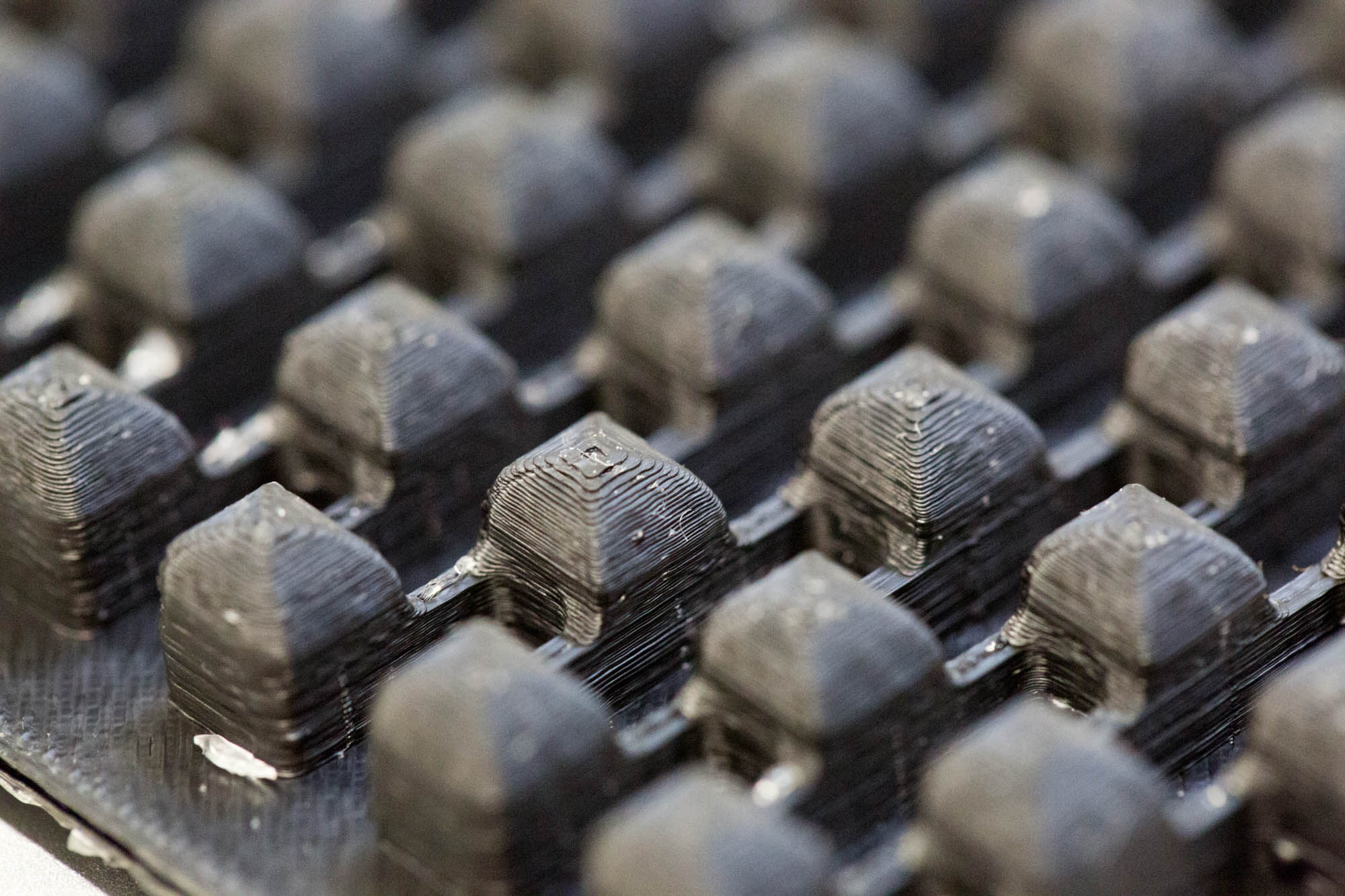
The mold designs were printed with a commercial 3D-printer (2nd generation MakerBot with MakerWare software; MakerBotIndustries, Brooklyn, US; 5th generation US$2'899) with acrylonitrile butadiene styrene (ABS, a copolymer of acrylonitrile, butadiene, and styrene). The maximum object size printable is [mm]: 225 x 145 x 150. The precision and minimum feature size are given as [mm]: 0.011 (XY-axis), 0.0025 (Z-axis); and 0.4 (XY-axis), 0.2 (Z-axis) respectively. The printing time varied with the size of the mold but was usually below 4 hours.
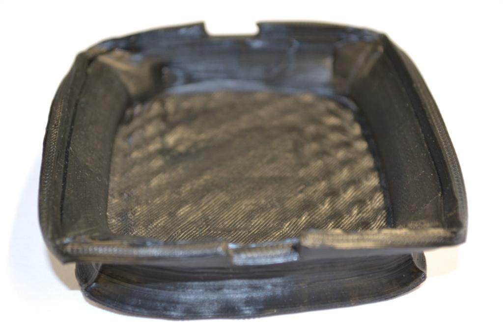
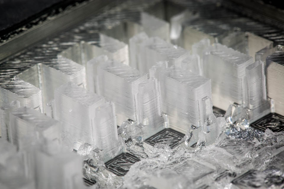
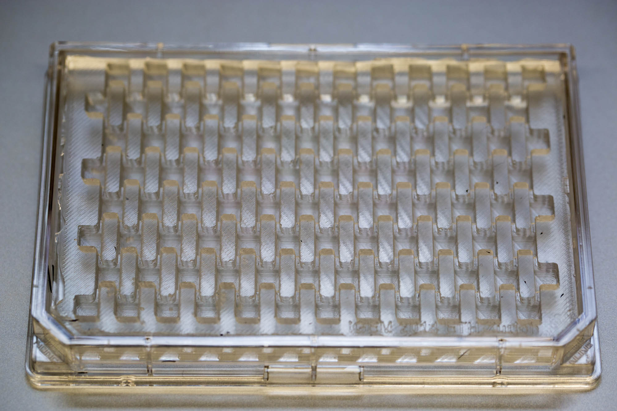
All fabricated structures were ready to use after removing the support structures and did not require additional surface treatments like sonication, curing, painting or silanization. The molds were then directly used for PDMS chip production. In addition, custom made black 96-well plates (connected wells for diffusion assays, plate reader compatible) were printed but found to be leaky over time. The material costs of the molds were in the range of US$2 to US$4 and for the 96-well plates below US$8 (about US$160 per kg of ABS). The maximum resistance to continuous heat is given as 90 degrees Celsius[23], as a result autoclaving at 121 degrees Celsius was not feasible (see picture below).
PDMS Chip Preparation
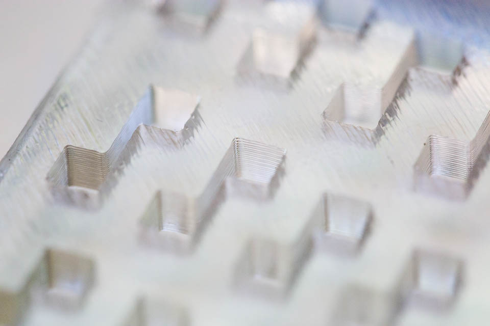
For the fabrication of millifluidic-chips raw PDMS (Dow Corning Sylgard 184) was prepared by mixing base and curing agent in 10:1 proportion. The PDMS solution was mixed vigorously and degassed (desiccator connected to vacuum) until no further bubble formation could be observed. Subsequently the mixture was poured over the mold and cured in an vacuum oven over night. The PDMS chip was easily removed without additional aids and placed in clear plastic trays (86 x 128 mm; OmniTrays, Thermo Scientific). The wells were then filled with CB medium and loaded with cells encapsulated in alginate beads.
Time-Lapse Movies
Imaging was implemented with a Biostep Dark-Hood DH-50 (Argus X1 software) fitted with a Canon EOS 500D DSLR camera and a fluorescence filter (545 nm filter). Pictures were usually taken every 2 min at an excitation wavelength (470 nm) with the standard Canon EOS Utility software. Time-lapse movies were created with Adobe After Effects CC software.
Below you find the time-lapse movies taken during the summer. In the very first trial the wells were filled with LB agar, holes were punched with a pipette tip and filled with highlighter-ink (pyranine) to visualize diffusion. Later, different set-ups were tested: chambers filled with liquid medium separated by solidified 2% agarose in the connecting channel and alginate beads in liquid medium.
We continued with the 'alginate beads in liquid medium' set-up, as it yielded the most promising intermediate results, and could then finally show cell-to-cell communication of bacteria confined in beads on our millifluid chip.
 "
"


